Saturday, June 23, 2012

NanoArt

Art is something that cannot be expressed with words. It is beautiful, but at the same time it will make you feel like its not, or it can just be random. It can make you feel happy, sad, or confused. Art is whatever you want it to be at a specific point in time. But most importantly, art communicates with you and sends you a message.


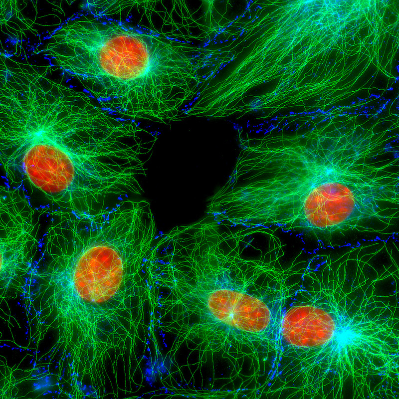
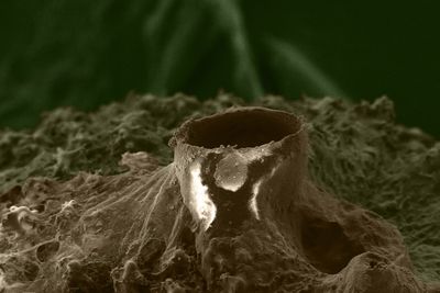
These characters are something that are pursued by scientist. One of the new types of art is nanoart. Nanoart alters atomic and molecular landscapes to build a type of art. Not only is it used for pleasure of the, but it is also used to raise awareness of nanotechnologies and to get young people interested in nanotechnologies. Here are a few examples of nanoart:


Nanometrology, Nanorulers, & Nanomanufacturing

Technology today is improving at a very quick pace. Every few months, a smaller thinner, more powerful version of a product comes out.
This rate is not going to stop, so technology is going to become much more powerful than before, but the workings inside the technology is going to have to change. It will need to become more organized, smaller, and most importantly, more precise.

Macbook Evolution
As it is, technology is precise up to the micron scale, but as technology gets small and nanotechnology becomes more and more banal, precision at the nano-level will have to be achieved. For that reason, nanometrology is an important sub-field of nanotechnology. Nanometrology is the study of measuring objects at the nanoscale. Easier said than done.

At MIT, the most precise, as well as the quickest way of measuring objects at the nanoscale is the nanoruler. The nanoruler not only measures distances, but it is used for grating*.  Normally, when technology businesses what to grate products at tiny distances, it uses a precise tool with a diamond point. The nanoruler actually moves the product the needed distance and then uses a laser to grate the technology. This is called nanomanufacturing.
(Source) (source)

"The Nanoruler can pattern gratings of lines and spaces separated by only a few hundred nanometers, or billionths of a meter, across a surface 300 millimeters in diameter. It does so with a precision of less than one nanometer. "That is the equivalent of shooting a target the size of a nickel in Manhattan all the way from San Francisco," said Carl G. Chen (Ph.D. 2003), one of Schattenburg's colleagues." (source)
MIT Stata Center
* grating is any regularly spaced collection of essentially identical, parallel, elongated elements


Nanomanufacturing is also defined as "the ability to fabricate, by directed or self-assembly methods, functional structures or devices at the atomic or molecular level," (p. 67) from the report  National Nanotechnology Initiative  (NNI) Instrumentation and Metrology for Nanotechnology. An example of this definition is of the new ways of building nanogears in which they can actually build themselves. (See Post on Nanogears)

Resource: Nanoforum

The Nanoforum is a website that provides the news on Nanotechnology. It gives information on new types of Nanotechnologies, big upcoming conferences, and projects and competitions for nanotechnology.

Sunday, June 17, 2012

Astronomy Section

The transit of Venus is over, but it gave me an idea on another post. This post will be describing the application of nanotechnology for the study of the largest objects, more commonly known as astronomy.

1) Graphene
As it turns out, graphene has yet another use. It has been conceptualized to use graphene as a way to protect spaceships from meteor debris and other substances that could cause corrosion of the ship. Due to its properties of being strong, flexible, cheap, and easy to make, it does not corrode, easily, thus protecting the spaceship.
(source)
Graphene sheet


Other than astronomy, this anti-corrosion property can protect objects on Earth from oxidation.

2) Space elevator
The space elevator applies carbon nanotubes to make  a shaft to let an elevator climb and get into space.
Nanotube Space elevator (artist's dipiction)
3) Telescopes: X-Rays
Wavelength of light chart
Above, is a chart that describes the wavelength of lights. Visible light is where there is the triangle  of colors in the middle of the chart. From the 10nm to the 10-3nm (10-11 meters) is a type of light called x-rays. X-rays are especially useful in astronomy. They help us take pictures of stars, detect properties of the stars and help us collect information on dark energy, black holes and neutron stars. Also, before the nanoscope was invented, it let us see things at the nanoscale, as particles at that size are to small to see with light. In other words, it lets us see things that a regular microscope can not see, like nanoparticles

However, due to the distance of the things we study in space, The changes are often very fine, and so very precise instruments are needed to detect these differences. Not only that, but the process to decipher the X-rays often takes a lot of time. 

Nanotechnologies can help by making tiny mirrors that allow scientist to use X-rays more practically and with greater precision. These mirrors can diffract light to the X-ray wavelength,thus making X-rays. The newly forged method of producing X-rays is called Critical-Angle Transmission or CAT.

4) Spaceships

The true heart and soul and astronomy is essentially astronomy.
Our current a space travels are abbord huge billion dollar investments. People are trying to make this price go down by using cheaper parts or changing design plans of the shuttle.
Saturn rocket take off
Russian Rocket ship
Shuttle rocket take off
Although these rockets seem to be totally different from each other, they have one core thing in common.

All these rockets are super-expensive projects that do not have a single mission to accomplish but a list of many tasked to accomplish while in orbit. In other words, we spend millions, if not billions of dollars to get these rockets into space to do lots of things.

There are two main things nanotechnologies can do to change this:

The first is quite obvious. Using nanotechnologies, we could make instruments on board smaller and more precise. We could also create a new type a fuel that is easier to make, cheaper, and more efficient by altering the properties of the fuel at its most basic level.


The second thing nanotechnologies could do is change the current goal of space ships. Why not create tiny little probes that do specific tasks, rather than these huge rockets that do many. It would certainly be less costly.

Even better, think about all the satellites that are in our orbit and how many are sent up each year. Now imagine that we send up a hundred or so tiny probes with each one. Each probe would the separate from the rocket, and make the rocket not only profitable to the business sending it up for business, but also profitable for science.

Monday, June 11, 2012

Copper-Nickel Nanowires

Ever wonder how the screen of an Ipad works. Me too, but I really don't know. This post, however, is just as interesting as that topic.

Copper-nickel nanowires might be the future of touch screens and for printable technologies. The nanowires are flexible and cheap and have the same properties as the current technologies in touchscreens (indium tin oxide, or ITO).

Another practical use of copper-nickel nanowires is that they can make solar panels much cheaper because it has all the necessary properties, is cheaper, and even more durable.


To start, indium tin oxide is the current leader in the field of touch screens. It is a substance that is good for touch screens because it is highly conductive (electrically) and is also transparent. However, it is rare and fairly expensive. 
Indium tin oxide glasses

A possible replacement was copper nanowires. Nanowires are wires at the nanoscale and are different from nanotubes because they are not hollow. Originally, when these nanowires were being created, it was found that after a little bit of use, the screen would actually become yellow, and then eventually green, like the statue of liberty. For obvious reasons, this type of screen was not put into commerce. However, recently at Duke University, a slight change to this original idea was made to solve some of the copper nanowire's problems.

Duke University creates the copper-nickel nanowire

Then the scientists thought about how pennies turned green, but not nickels. By adding nickel into their nanowires, they were able to take off many of the problems from the copper nanowires. One such advantage that was created by adding nickel was that it lost 50% of its conductivity in 400 years, much more than the indium tin oxide screens.Unfortunately, this new cheap alternative will probably not replace its predecessor for a simple reason; it cannot yet conduct enough electricity for our common day-to-day technologies.

Even though this is a big issue of the copper-nickel nanowires, it would be quite biased to ignore the possibilities presented with the Copper nanowires. Copper nanowires can be used in printable technologies because it is flexible, cheap, and durable. This printable technology can be used for for shipping boxes to scan it, in magazines, and much more. 
Copper Nickel Nanowires


It can also be used  as a way to make interactive clothing, which is a very tangent to this topic, but interesting none-the less.

Tuesday, June 5, 2012

Transit of Venus

Today is a big day for the opposite of nanotechnology; the study of huge things, or more specifically, astronomy.
Today, there was a transit of Venus in front of the sun. This means we got to see venus' shadow from Earth. It will be the last time for 105 years that this happens. Personally, I did not get to see it because of heavy overcast here in New Jersey, but I hoped everyone else that could enjoyed it.

Sunday, June 3, 2012

Graphene

What do we think of when we are told '2D'? Normally we think of paper or a '2D drawing', even though we know that neither paper, nor drawings are really one atom thick.

The discovery of graphene is one of the most impressive discoveries within the realm of nanotechnologies. Graphene is one atom thick, and is surprisingly easy to make. Essentially it comes from graphite, or more commonly known as pencil lead.

Gaphene is a type of carbon atoms with the formation of sp squared , which is a hexagonal formation.
Hexagonal carbon formation
Graphene is a significant discovery because it opened up the ideas, to not only 2D planes, but also 1D lines like nanotubes, and even 0D points, which are essentially atoms.

Graphene is also a big contributor to the progress of technology because of its properties. It turns out that graphene is a great conductor of electricity-its 2D qualities make electricity pass through it even faster than regular graphite, which was a good conductor to begin with. This means that it can, and will be, used in electronics to make them fast. Not only that, but it is flexible, which means it can create flexible technologies. It also is incredibly strong, even with its flexibility.

Nanogears

What is one of the most basic tool for machines to move things. The answer: Gears.
One of the newest inventions in nanotechnology, nanogears hope to create molecular-machines. They will do so in the same exact way as regular machines - just, tiny.

In the past, nanogears were created by using a laser to carve the gears. This process took up to much time to be able to get nanogears cheaply, or use them efficiently for molecular machines. Columbia university solved this problem by making nanogears that can assemble themselves. The scientist did that by putting a sheet of metal, like copper against a polymer sheet. Due to the properties of polymer, it shrinks faster than the copper sheet when it cools, thus making evenly spaced teeth in the polymer, creating a nanogears.
(Source)
However, what is the point of having these gears if they do not turn or create change? Fullerene nanogears (1st video above) are turned when a beam is sent  down the nanotube (which is what the nanogear is center is made up of) creating an electric field around the tube. "A positively charged atom is placed on one side of the nanotube, and a negatively charged atom on the other side. The electric field drags the nanotube around like a shaft turning". Source

Saturday, June 2, 2012

Contact: Dr. Anthony Novembre

Dr.Anthony Novembre
Industrial Outreach Coordinator of PCCM at Princeton University.


Anthony NovembreAssociate Director
Princeton Institute for the Science and Technology of Materials
Princeton University
70 Prospect Avenue
322 Bowen Hall
Princeton, New Jersey , 08540-5211
Phone:             609-258-6855      
Fax: 609-258-1177
Email: novembre@Princeton.edu

Contact: Daniel Steinberg

Mr. Daniel Steinberg,

Director of Education Outreach for PCCM (Princeton Center for Complex Materials) at Princeton University. Mr. Steinberg works to reach out to students at any level and get them interested in material studies.


Phone: (609) 258-5598
Email: dsteinbe@princeton.edu