Monday, December 21, 2015

Northwestern University Center for Cancer Nanotechnology Excellence (CCNE)

Northwestern University has been a leader in nanotechnology and is becoming a powerhouse for the propagation of the technology to the clinical market. Many research insitutions are great at discovering new materials, but it is rare that one works so closely with the market to not only innovate but apply new discoveries.

A major reason for Northwestern lies in both its support of nanotechnology research and in the funding its been receiving. Its Center for Cancer Nanotechnology Excellence has just received 11.7 million dollars from the National Cancer Institute (NCI). The reason why Northwestern is such a great player in nanotechnology research is that it is not only immersed in just nanotechnology, just medicine, just biology, or just physics and engineering. Instead, it is an integrated research institute. This is so important for nanotechnology research as this field doesn't settle easily into any one classical discipline. Instead, it requires the application of many different expertise.

Northwestern, in particular, claims that its International Institute for Nanotechnology and its Robert H. Lurie Comprehensive Cancer Center of Northwestern University will be able to work together to create nanotechnology and then streamline it in-house to clinical research and, eventually, the clinical market.

An image of NanoFlares
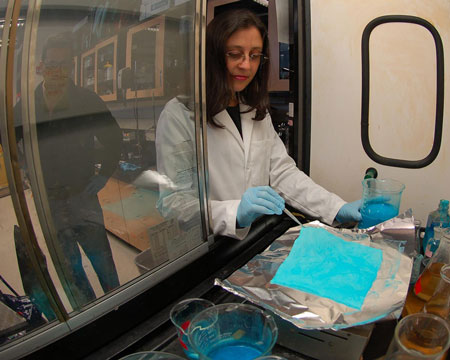
Currently, the flagship of Northwestern's research is in its NanoFlare (see image right).  NanoFlares are a "spherical nucleic acids with gold nanoparticle cores outfitted with single-stranded DNA “flares.”". The NanoFlares expand upon nucleic-acid based Nano-constructs called Spherical Nucleic Acids (SNAs) which are non-toxic to humans and can serve in the delivery of cancer drugs. What makes the NanoFlares unique is the DNA-flare on the outside of the sphere. It allows the SNA to locate and bind to cancerous cells in the blood stream even before any tumor forms. Then, a drug can be released to destroy the harmful cells.

This research is not only important in the fight against cancer but is a clear demonstration in academia embracing nanotechnology and seeking ways to maximize its impact.
To read more about the grant and Northwestern's research, click here!
To read more about this research, click here!
To read more about the International Institute for nanotechnology, click here!


Monday, December 7, 2015

Superfast fluorescence sets new speed record

The device you are currently sitting on, whether it be a phone, a tablet, or a laptop, is at its core made of a tiny switches that are turned on and off by electrons at extremely high rates. These 'on' and 'off' states are what occur when you look at the base of a code and see a 1 - on - or a 2 - off. As technology improves, however, we are reaching the limit of how fast these switches can be turned on and off - that is, the passage of electrons through wires is no longer fast enough. Currently, we solve this in personal laptops by making the switches smaller and adding more of them. In supercomputers, we cool the computers down and use rare metals to create superconductors; thus decreasing the resistance of the wire for the electrons and increasing the electrons velocity.

This sort of improvement, however, is finite and innovation is needed. Although one up-and-coming and viable option is quantum computers (discussed in other blog posts) another is to change the medium through which we manipulate the switches. This is to say, replace electrons with something that moves even faster: Photons.

This, unsurprisingly, has certain barriers to overcome before it can become a reality. Optical computing, fortunately, has come one step closer to reality with an innovation made by the Pratt School of Engineering at Duke University. There, researchers have created a light source that can switch on-and-off 90 billion times per second using plasmonics. Plasmonics occur "When a laser shines on the surface of a silver cube just 75 nanometers wide... [then] the on its surface begin to oscillate together in a wave. These oscillations create their own light, which reacts again with the free electrons. Energy trapped on the surface of the nanocube in this fashion is called a plasmon."

After thus exciting the silver nanocube, the electromagnetic field created  reacts with two layers that are nearby: a gold sheet ~20Agstom away and a quantum dot layer that is placed between the silver nanocube and the gold sheet. The quantum dots in this middle layer emit light that can be turned on and off 90 billion times a second.

Clearly, this is an innovation that will be of service to even the average consumer. It is yet another example of how influential and important nanotechnologies will be in our future.
To learn more, click here!

Monday, November 23, 2015

NanoViricide

Pesticides, it seems, is part of our everyday lives as we try to kill that buzzing mosquito in the corner of the room. However, it is also a technology that has been able to increase crop yield and feed millions of people by eliminating insects that eat or infect crops. Similarly, Nanoviricide is a company that is trying to create the equivalent result against viruses.

To understand their technology, it is important to first understand the structure of a virus. As seen in the diagram to the right, a virus is primarily made up of three components: The Genetic Material, the Membrane Envelope, and the Ligands. The first of these three is stored on the inside of the virus. Once the virus attaches to the cell, the DNA or RNA enters the cell and eventually takes over the cell's machinery. Thereafter, instead of producing normal proteins needed for cell function, the cell produces copies of the virus until the cell no longer has enough nutrients to live and dies. The second of these, the membrane, protects the genetic information when the virus is not in a cell. The last is what NanoViricide attempts to take advantage of:

Simply put, the ligands on the virus are made such that they bind with the surface of the cell. NanoViricide thus creates a delivery capsule that mimics the virus's corresponding ligand, causing the virus to attach to the NanoViricide. Once this is done, the Virus can be easily killed.

The company has used its technology to help fight viruses such as HIV, Influenza and Bird Flu and shows an important use of nanotechnology in medicine.
To learn more about NanoViricide, click here!
To learn about the entry of the virus into the cell, click here!

Monday, November 9, 2015

Northwestern's induction into the Center for Sustainable Nanotechnology

Through all its benefits, the community at large is making sure that new innovations through nanotechnology do not hurt the environment. To this extent, the NSF provides $20 million (renewable) to centers of research that research the effect of nanotechnologies. The funding is provided to the Center for Sustainable Nanotechnology, who very recently has inducted Northwestern University into its group of institutions.

Some of the big questions they're asking include:
How is this going to impact bacteria and other organisms in the environment?
What do these particles do?
How do they interact with organisms?”

The goal is to create nanotechnologies that will not hurt the environment in the first place so that later recalls due to environmental hazards won't be necessary. To this end, there is both an environmental and an economic motivation to ensure that we have the knowledge on the impacts of nanotechnologies. It is part of a movement for our society's businesses and corporations to be more environmentally friendly.

To read more about Northwestern's induction into the society, click here!

To read more about the Center for Sustainable Nanotechnology, click here!

Monday, October 26, 2015

Phys.org

Phys.org is a website that provides news for all types of sciences, including:
  • Nanotechnology,
  • Physics
  • Earth
  • Astronomy and Space
  • Technology
  • Chemistry
  • Biology
  • and More!
It is a great news agrregate that, unlike many other science magazines, offers a full page for nanotechnologies. If you want to get the best and newwest in nanotechnology or any of these other science, this is a great source. Click Here to visit Phys.org

Monday, October 12, 2015

Stanene

One of the hallmarks of nanotechnology is graphene, a two-dimensional sheet of graphene with unique heat conducting, electronic, and strength properties. However, graphene is not the only 2D material in existance; others include silicene, phosphorene, and germanene.

Recently, a new member has been added to this list: stanene. An allotrope of Tin (the term Stanene is derived from the latin word for tin Stannum), Stanene is two hundred times stronger than steel and has the unique electronic property of conducting electricitiy without creating heat.
A Diagram of Stanene

To start, the structure of stanene is similar to graphene: a hexagonal grid structure that is a single atom thick. However, unlike graphene, it has ridges, meaning that if you were to look at it from the side, it would look like a zig zag. It is along these ridges that electrons are able to run through the substance (thus conducting electricity) without interfering with any of the interior electron and, thus, without losing any energy to heat. At least theoretically.

Stanene, though 'tested' theoretically be able to exist and have certain properties like the ones outlined above, the material hasn't definetively been created. Although researchers Shanghai Jiao Tong University claim to have created the ultra-thin sheet by vaporizing tin and having it deposit on a bismuth telluride surface, some critisize the finding due to poor imaging and a suspicion that the bismuth telluride surface interacted with the tin atoms to create an impure surface.

Currently, more work needs to be done to confirm the current findings or develop a new technique to create stanene properly, but there is certainly promise for graphene to have a star for a cousin.
(Source)

Monday, September 28, 2015

Sonoplot

Sonoplot is a company that has developed a nanomaterial-printing technology. Using it's "microplotter" it is able to dispense tiny volumes of material onto surfaces using a pen that uses an ultra-sound pump to dispense the liquid.
Image of a plate printed by Sonoplot's technology
Working with a more varied series of fluids (including more viscus ones) and higher resolution of deposition than its current competitor (the inkjet printer), the microplotter may allow for the utilization of nanomaterials' (like carbon nanotubes) properties in a controlled and effecient way.
Diagram of an Inkjet Printer

The reason for the microplotter's versatility is its patented ultrasonic pumping action. Unlike an inkjet printer that works by popping tiny volumes of inks onto paper in dots of 50-60 micrometers (details for the process on how an inkjet printer works is outlined here, and shown in the image to the right), the microplotter deposits the material directly, as shown in this video.

Sonoplot, the manufacturer of the microplotter tells about the promise its technology holds for smaller, cheaper, electronics. However, one can easily imagine further applications for this type of technology; be it property testing or fun drawings!

To learn more about the sonoplot's technology, click here.

Saturday, September 5, 2015

WIN Seminar - Dr. Aaron Wheeler: Digital Microfluidics for Three Dimensional Cell Culture and Single-Cell Signaling Assays

For those of you interested in Nanotechnology and in learning more about it, Dr. Aaron Wheeler, a professor at the Univeristy of Toronto will be giving a seminar about research in nanotechnology (abstract below).

"Digital microfluidics is an alternative to microchannels for fluid handling in which discrete droplets are manipulated electrodynamically on the surface of an array of electrodes covered with a hydrophobic insulator. In this talk, I will describe two projects in which we are exploiting unique attributes of digital microfluidics to enable mammalian cell culture and analysis. In the first project, we have developed a system for generating arrays of microgels “on-demand” with arbitrary shapes and contents. We have used this system to identify conditions that control 3D kidney epithelial spheroid formation. In the second project, we have developed a system that allows for quantitative immunocytochemistry assays in adherent cells at the single-cell level. We have used this system to screen for PDGF signaling events with high time resolution. These examples are representative of interesting new possibilities for cell culture and analysis and other applications that are enabled by digital microfluidics. I will also briefly review our efforts to make these possibilities accessible to all users via open-source hardware and rapid prototyping techniques."


The Seminar will be given at the Quantum Nano Centre (QNC) in room 1501 on September 17th at 3pm
200 University Avenue West
Waterloo, ON N2L 3G1
Canada     

To learn more, click here!

Sunday, August 16, 2015

Nanotechnology 101: The Biggest Thing You've Never Seen

As Nanotechnologies continually change the world and our lives, it is one of the goals of the Royal Institution (RI) to give awareness about how nanotechnologies will further be able to change the way we live our lives.

To this end, the RI is hosting Michael Meador, the Director of the U.S. National Nanotechnology Coordination Office that was created under NASA. In his talk at the RI, he will be discussing the following topic:

"How could nanotechnology be used to create smart and extremely resilient materials? Or to boil water three times faster? Join former NASA Nanotechnology Project Manager Michael Meador to learn about the fundamentals of nanotechnology—what it is and why it’s unique—and how this emerging, disruptive technology will change the world. From invisibility cloaks to lightweight fuel-efficient vehicles and a cure for cancer, nanotechnology might just be the biggest thing you can’t see."

The event will take place at the Royal Institution Theatre, located at: 21 Albemarle St, London W1S 4BS, United Kingdom

Admission Prices
Standard: £12
Concession: £8
Associate: £6
Free to Members, Faraday Members and Fellows

Sunday, August 2, 2015

NanoTechnology in School

Since the inception of this blog, the perception nanotechnology has changed dramatically in the field of education; especially in university. More and more institutions are increasing budgets for research on nanomaterials and nanotechnologies, and more researchers are becoming aware of the useful and unique properties seen at the nanoscale.

As recognition of its importance, some secondary-level schools are beginning to question how they should go about pursuing the education of nanotechnology to students. Some believe that nanotechnology should be taught as its own class in school, much like physics or chemistry. Others, however, believe that, due to the wide scope of nanotechnology and its application in many of these fields, nanotechnologies should be incorporated into current courses as additional material.

Currently, there are attempts to fill the void that exists by the lack of any education. Some of these include nanotechnology summer camps, which introduce concepts, techniques, and technologies to high school students, and course kits that teachers or parents can order online to use as teaching aids for their students. Additionally, some schools and foundations like the NSF (national science foundation) encourage students to visit their labs and explore this new realm.

What do you think on this debate? Should a class be created in high schools for the sole purpose of teaching Nanotechnologies? Leave a comment below!

Smart Nano-Fibers

Over the last several years, there has been much excitement in the world of technology concerning the integration of electronics into clothing. However, there has been significant difficulty in achieving this goal as electronics that are woven in in addition to fabrics become heavy and inflexible, causing discomfort and uneasiness for use. However, the Hinestroza Lab at Cornell University has been able to manipulate cotton fibbers at the atomic level to create fabrics that have electronic-like properties. This means that instead of adding electronics to fabrics, the fabric becomes an electronic.

The benefit of this is that the resultant clothing remains light, flexible, and productive. The team has already created  a dress that has ultrathin solar panels that can charge a cell phone. This type of technology holds promise as it could surely be used to keep you online when you away from home or to track your movements, or do much more.
To find out more, click here.

Water Purification through Synthetic, Animal-Like Membranes

According to the Rehydration Project (source), 1.8 million people die of dehydration each year, due to a lack of drinkable water. Of these, 90% are children. A possible solution for this problem might come in the form of filters with pores so small that only water molecules (and not other large particles nor cells) can penetrate. This has been achieved before using carbon nanotubes; however the difficulty to produce and align the tubes has led to a continued need for innovation.

An international team of researchers, including some from Penn State, has used bio-mimicry of cells to help solve this by making a synthetic, self-assembling membrane.

The reason for this is that cells, which have a fat-based phospholipid bilayered membrane, are able to control what enters the cell due to its membrane (diagrammed below). A cell, however, required water and certain proteins, and regulates the entry of these using transport proteins, which span the length of the membrane and provide conditions that allow specific proteins and molecules to travel through. Cells have a specific transport protein called aquaporins that create a channel that allow water to enter or exit the cell through osmosis. However, it does not allow other proteins or molecules to enter with the water; effectively acting as a filter. 
Diagram of a cell membrane
It is this property that the researchers were interested in. By creating a synthetic cell-like membrane equipped with aquaporin like protein channels, they have created a method whereby water transmutes through the membrane at extremely extremely high rates (1 billion water molecules per second, per channel) that is also able to be created quickly and more cheaply than earlier iterations of synthetic membrane-filters. This innovation could thus prove to be a very beneficial one by giving access to water to communities who lack it.

Sunday, July 26, 2015

NanoMedicine: Fighting Heart Disease

According to the Center of Disease Control (CDC), the leading cause of death in the United States is Cardiovascular disease, which claims approximately 611,000 lives per year and includes symptoms like Myocardial infarctions (MI) (Heart attacks) (source). Heart attacks occur when an artery in the heart becomes blocked - often through blood clots that form when atherosclerotic plaque (caused by an unhealthy diet) ruptures - as explained in the Ted-Ed Video here.
How blood pressure works - Wilfred Manzano - Ted-Ed

Due to its high prevalence in advanced countries, much research has been done and many drugs developed to help treat the disease. Nanotechnologies have been developed, at the Laboratory of Nanomedicine and Biomaterials at Brigham and Women's Hospital in Boston, USA, that may  aid in the treatment of this disease by aiding in the delivery of  cardiovascular drugs directly to the atherosclerotic plaque sites. Specifically, they developed  a 'nanodrone' that was able to attach to the plaque and deliver the drug Annexin A1, which resulted in decreased inflammation, decreased plaque size and increased thickness of the collagen layering the plaque (helping prevent plaque rupturing and blood clotting) in mice. The result was that mice that relieved the treatment of the drug did not experience an MI. Moreover, when the same drug was administered without the nanodrone, the treatment was ineffective, as when the nanoparticle was administered without the drug.
A Depiction of the 'Nanodrone'
Clearly, the application of nanotechnologies for delivery of drugs is a serious one that will help make treatments more effective even outside this specific example. It shows that nanotechnology will enhance modern medicine and help improve the quality of human life, which is one of the ultimate goals of technology and medicine. 

To find out more about cardiovascular disease, click here.
To find out more about Myocardial infarction, click here.
To find out more about this nanotechnology, click here.

Graphene: The World's Thinnest Lightbulb

Graphene has long been acclaimed by popular media that covers nanotechnologies because of its ever increasing number of unique properties and applications - including  extraordinary strength and conductibility. Recently, researchers at the Seoul National University, the Korea Research Institute of Standards and Science, and Columbia University have added to graphene's impressive resume when they developed a light bulb with a graphene filament that was an atom thick.

Previously, extremely small filaments like this were not feasible because the filament would have to be heated to exorbitant temperatures that, even if they didn't melt the filament, would melt the surrounding materials. Graphene, however, offers a solution to this, as it harbors the property of being less conductive of heat the hotter it gets. This thus allows graphene to be heated to temperatures that allow for light to be produced (~2500C), while maintaining the structural integrity of itself (due to its inherent strength) and its surroundings.

Furthermore, graphene - being and incredibly thin substance - is effectively clear, meaning that light can travel through it. The researchers found that (due to this) one is able to alter the wavelength of light emitted by the graphene light by changing the distance between the graphene filament and its silicone substrate, as see in the video here.
The advent of this type of light will advance technology because it is both flexible and small, meaning it will be able to be integrated in flexible technologies and displays, as well as on small chips.

The researchers are currently working on methods for turning the bulb on and off, but perhaps there will soon be a day when graphene will revolutionize the technology of displays! 

Saturday, July 25, 2015

Nanotechnology Could Cure Teenage Acne Forever

Acne is a skin infection that occurs when skin pores get congested, often with a naturally occurring, oily lubricant called sebum - created by the sebaceous gland. During adolescence, when the skin in changing, many teenager's sebaceous glands over produce sebum, leading to congestion, infection, and, ultimately, acne.
Diagram of a Normal Follicle
Most modern treatments of acne work by treating the symptoms of the infection or by trying to diminish sebum production chemically. Often times, these drugs also cause unwanted side effects - like skin dryness - or resistance. However, researchers at University of California at Santa Barbra, have developed a possible alternative to current treatments. Rather than a purely symptomatic treatment, they have utilized nanotechnologies to directly destroy the over-productive sebaceous, thus stopping the production of sebum and curing the resulting acne.

More precisely, the drug is a silicon oxide molecule with a gold encasement in the nanosize region. It's size is particularly useful for its delivery as it is able to enter the pores transdermally - that is, without injection or consumption.

The treatment has three phases, illustrated below. The first is to apply the nanoparticle formulation to the skin. The second is to use low-frequency ultrasound to 'push' the nanoparticles into the follicle - this is the delivery system. The last step uses a laser to activate the treatment and effectively cure the acne.
A Diagram of the Phases of the Nanoparticle
The final step works through a process called Surface Plasmon Resonance (SPR). Illustrated in the diagram, SPRworks when a beam of light is shined at a metal surface and the light resonates with the metal in such a way that a specific wavelength is converted from light energy to mechanical energy or heat - as seen below with the "plasmon wave".

The researchers used this property of metal in their nanoparticle. Once the nanoparticles have entered the follicle (the second phase), a laser (which is a beam of light at a single wavelength) is pointed at the targeted area. Due to the particle being a metal, an SPR effect is created, leading to heat production that deactivates the overactive sebaceous cells.

Diagram of Surface Plasmon Resonance
Although the treatment is not yet in the market, it is currently undergoing clinical studies, where side effects and efficacy are being studied.

It is clear that the work on this drug has not only been useful for the treatment of acne, but has also provided for a new delivery system (via ultrasound) and proves to the world the eminence of nanotechnologies.

To learn more about the treatment, click here.
To learn more about Surface Plasmon Resonance, click here.

Nano3D Printing

3D Printing is a subject that has become of high interest to engineers and stockholders alike. It holds the promise of revolutionizing manufacturing, product development and innovation, the delivery of goods, and, overall, the way we live our lives. Yet, somewhat unbeknownst to the popular audience, the technology is also making strides at the nano-scale.

To begin, 3D printers at the macro scale turn digital blueprints or designs into a reality by breaking apart the 3D design into 2D layers and then stacking these 2D layers on top of each other to make the object.

This can be analogized to the volume (3D) of a cylinder:
It is well known that the formula definite a cylinder's volume is πr^2*h, and if you break this formula down into its component parts, you see that there is πr^2 and the height. Furthermore, the equation implies that you have the area of a circle the height times to get the volume. It's as though you have CD disks - the area being one CD and the height being the number of CDs. The volume of a stack CDs would be the area of one CD times the number of CDs (this works assuming you know the height of a single CD, but in a cylinder, the height of the disk is null, thus we multiply by the height directly, not, say, the number of disks or circles).


Thus, by applying the many near-2D layers, a 3D figure is created. Furthermore, the resolution is dependent on the thickness of each layer. For example, if you have a curve (the red line below) that you are trying to recreate, but can only do so using rectangular bars, you can clearly see that the thinner the bars, the more smooth a curve you can make - the same is true in 3D Printing.

When we move to smaller scales, this resolution becomes a limiting factor, and, as a result, new innovative techniques are required to maintain high resolution and high speeds.

The Vienna University of Technology has created a new method for 3D printing that overcomes some of these limitations called two-photon lithography.
Two-photon lithography is an evolution on [one] photon lithography, which uses the property that some liquids, when exposed to certain photons, solidify. Thus, by accurately firing photons at a liquid sample (often using a laser), one is able to 'carve' a solid. After the solid is carved out, the remaining fluid is simply washed away, leaving behind only the finished product.

Two-photon lithography expands on this by using resin - a viscous fluid - doped with other molecules, which solidifies when two photos hit it at the same time. This means that two different light sources are used and the solid is formed only where those two intersect in the resin. The benefits of this are 3-fold: the precision and resolution are increased (as the area of intersection is so small), the speed is vastly increased (from millimeters per second to five meters per second), and the printing no longer has to occur layer by layer (the photons can intersect anywhere within the resin to make a solid, not just the surface, as in traditional macro-3D printing and single-photon lithography).

Thus, overall, the team created a much faster, versatile, and high-resolution 3D printing method than has existed before. The team exemplified the technology's capability through this video of the creation of a 330 x 130 x 100µm^3 size F1 race car, seen here.

This innovation is a major step forward in nanoscience because of its possible application in cell biology, immunology, nanotechnology-manufacturing, and fields that have not yet even begun to be conceived.

To find out more about two-photon lithography and this team's project, click here
To find out more about 3D printing in general and the various types of 3D printing, click here

Wednesday, July 8, 2015

Nanotechnology Student Video Project

As Nanotechnology gains momentum, many are starting projects to raise awareness in the general community, not only about the field, but the importance of nanotechnology. The National Nanotechnology Initiative, supported by the government, sought to do this by creating a student video project wherein college age researchers could present their research projects in a way that the general audience could understand and appreciate.


Its first prize winners were Abelardo Colon and Jennifer Gill for their video on the application nanodiamond powder for the purification of water. Their proposal for nanodiamond purification or water was a solution to the chlorination process used today that creates harmful byproducts. Their method was more effecient at killing bacteria, was reusable, and did not cause such harmful byproducts as the methods currently used. (Source)

NanoTechnology World Association

Created recently, the NanoTechnology World Association is a website who's goal is to close the gap between researchers and markets, and increase awareness of Nanotechnologies to accelerate its entrance into the market.

The site analyzes area's of development for nanotechnologies, provides news about nanotechnology and its innovations, and aggregates upcoming worldwide events in nanotechnologies like "Nanotech France 2015".

Though new and still in development, the project will certainly spread knowledge of the field to both markets and consumers.
(Source)

Kabiller Prize in Nanoscience and Nanomedicine

At the start of this blog, five years ago, nanotechnology was a field that few had heard about but was growing at an astonishing rate. Now, many universities are focusing on nanotechnology and nanoscience, as seen with the construction of new Nano-facilities like Princeton University's Nano-Fabrication Laboratory.

Source
In recognition of the outstanding developments in nanoscience and its importance in medicine and health, a leader in Nano-medicine, NorthWestern University's International Institute for Nanotechnology has created the international "Kabiller Prize in Nanoscience and Nanomedicine", who's goal it is to "recognizes researchers who have made exceptional advances in nanotechnology and its application in the field of medicine and biology, that have the potential to improve the quality of life for future generations." Due to the generosity of David G. Kabiller, the honor is awarded biennial with a $250,000 prize.

In addition to the "Kabiller Prize in Nanoscience and Nanomedicine", the same fund also provides for the $10,000 "Kabiller Young Investigator Award in Nanoscience and Nanomedicine", targeted to highly accomplished researchers within 20 years of earning their degree.

The first recipients of the awards will be announced in August of this year in a ceremony that will include prestigious speakers like 2014 Nobel Prize Chemistry winner William E. Moerner.

For More Information: (Source)(Source)

Monday, March 16, 2015

How small is the Nanoscale?

What could a stadium-sized bowl of peanuts, a shrinking elephant, and a crazed hockey player have to do with nanoscience? Those are just a few of the goofy excursions that await you when witty host Adam Smith and wacky physicist Ivan Schuller take you on an irreverent, madcap, comically corny romp into the real-life quest to create the smallest magnet ever known. 

This funny video (20 mins) restates the orders of magnitudes that characterize the nano-scale. It is a good introduction (and perhaps mandatory viewing !) for the new readers of my blog, as I often assume that everyone is comfortable at zooming below the micron into the "guts" of a cell, or basic architectural structures of a crystal.

Enjoy this video, and the blogs posted here.


Monday, February 23, 2015

Upgrading from microscope to nanoscope

There is an increasing amount of academic and industrial research and applications development around the nano-scale, and the market of nanoscope is really growing. But these systems are not cheap: the acquisition of a super-resolution system costs several hundred thousands dollars, without mentioning the cost of laboratory real estate and trained personnel.

In addition, what are the real possibilities of optical systems ( who operate with visible light in the 400nm - 800nm range) to resolve nanoscopic features in the 100 nm range ? How can "400nm photons" see features that are smaller than them ?


Sophisticated confocal microscopes can achieve excellent resolution of 250 nm to 500nm depending on their cost (in particular related to the laser system, the optics, the detector and the computing capabilities to capture and "stack" and process many images) in the X and Y dimensions. In the Z dimension, the technology has much less resolution.  The installed base of such microscope is huge, and there are many good manufacturers. Every decent life-science lab has one, plus all the surrounding accessories, trained users and all the related image analysis tools.

In this blog, we would like to show you how two manufacturers are marketing upgrades (or "add-on") systems that use very astute approaches to improve the resolution of a confocal microspcoe by a factor ot 1.5 to 2, hence reaching the ~100nm limit.

Airyscann from Zeiss
In the middle of 2014, the German company Zeiss has launched a "add-on" system that  plugs into the optical port of their confocal microscope (picture to the right).

In addition to an improved laser beam management system, the big idea in this upgrade is to use a totally new concept of detector (camera). Instead of using a full field camera to capture the signal emitted by a sample illuminated by a very narrow light source (pinhole), Zeiss has introduced a detector that has a honeycomb structure (like a bee's eye): each of the  32 channels (each element of the honeycomb detector) collects all light of an pattern simultaneously. Each detector element functions as a single, very small pinhole. Knowing the beam path and the spatial distribution of each AiryScan pattern enables a very light efficient imaging: you can now use all of the photons that your objective collected ! Further signal deconvolution and image treatment enables resolutions in the ~150nm range !

The resulting images show features with much better resolution, enabling users to investigate (basically "see") features and events that they could not see below. For "only" $150k, many new questions can be answered ! ( Another way to look at it: imagine how many new cool internships for high-school can be generated!)


This is an example of the higher (X1.5 times) resolution obtained on the Zeiss confocal microscope equipped with the Airyscann upgrade)


CODIM100 from Bioaxial
The young French company Bioaxial is addressing the same opportunity with a totally different approach. As opposed to Airyscan where the trick resides in a multiplexed detection system, the investors at Bioaxial are using the properties of bi-axial crystals to "split" the light depending on the incoming polarization of the photons.  In short, the upgrade system contains optical elements that can split and shape the laser bean before it goes through the sample. When very high voltages are applied to the bi-axial crystal, several outcomes can be controlled, and the deconvolution, addition, subtraction of the images captured on a conventional detector can resolve features that are smaller to the typical resolution of the confocal microscope.

This is well illustrated in the two figures below:


The company is not fully commercializing its product yet in the US, and we do not know the price of the upgrade, but it will have to be in the $150k range to compete with Zeiss's Aryscan unless it brings significant differentiated value ( seem they are very gentle with the substrate, and do not damage it with the lase beam).

Their images are very nice as well:


In conclusion, we see that the market for upgrades of confocal microscopes to increase their resolution ( to ~100nm- 150nm at best in X and Y) is growing with new players and very astute ideas. This systems will not replace real super-resolution nanoscopes ( ~50nm resolution) , but the ticket to acquire such upgrades ( ~$150k) is VERY attractive. I cannot wait to put my hands on one of these systems.


Monday, February 9, 2015

The Toolbox of Nanotechnology researchers

What is the "toolbox" of a nanotechnologist ? I started tobuild my own list until I found the perfect answer on the webpage of the National Science Foundation's Material Research Science and Engineering Centers (MRSECs) Shared Facilities.

The Materials Research Facilities Network is a nationwide partnership of the Shared Experimental Facilities (SEFs) supported by the MRSECs. The MRFN is designed and operated to provide support to researchers and experimental facilities engaged in the broad area of Materials Research in academic, government and industrial laboratories around the world.

Every line on this list his linked to the related center (U.S. Universities) that can provide access to such tools.


Types of equipment

Friday, January 30, 2015

What do Europeans think about Nanotechnologies?

What do Europeans think about Nanotechnologies ? 

That is the simple question that was asked in a survey of 8,330 persons (out of 15,000 engaged). The initiative, funded by European Commission's Framework for Research and Development FP7, tested knowledge, willingness to buy, and perception, tested the European countries preparedness to adoption nanotechnologies. Data can be segmented into employment status, age groups, educational levels, and country.

Such a survey is important because it forms a foundation on the popular level of knowledge concerning nanotechnologies for European policy makers. It is also a great tool to measure trends in Europe.
The data can be visualized on the website's interactive map.


So what do we learn ?


UK is the country that is the most aware of NT 

(5 correct answers on a Quiz of 5 questions)


Poland and Greece are the two countries who are most ready to buy Sunscreens containing nanomaterials.


However, they are also the one's who know the least about nanomaterials.


Spain and Austria are the two countries that support the use of nanotechnology the most,

 but were the least likely to buy sunscreen containing it
(... but not to buy sunscreens....)


These three examples show the complexity in the relationship between how people percieve nanotechnologies, and how they actually react to partaking in it in common products
This complexity is why there is no conclusive result to all the data, but it is still valuable information. 

What do Americans Think About Nanotechnology?
This feature is even more interesting because it shows a vast development since the 2009 research, in which the american public in 2009 was almost completely unaware of the science and its applications. In the same year, groundbreaking poll of 1,001 U.S. adults, conducted by Peter D. Hart Research Associates and the Project on Emerging Nanotechnologies (PEN), found that 90% of Americans think that the public should be better informed about the development of cutting-edge technologies.

The Public Awareness of nanotechnology has barely moved over the last four years, despite huge efforts (funding, research, outreach initiatives, emerging new products etc...). This  is probably due to the lack of exposure of nanotechnologies in our daily life, and because they are not exposed sufficiently to high school students.

Which brings us to the mission of this blog.

Happy reading!