Sunday, November 18, 2012

NanoComposix

NanoComposix is a business who is rapidly growing and is thriving in the nanotechnology sector of business. It makes silver nanospheres, silver nanowires, silver nanoplates, silver silica Coatings, gold nanoparticles, silica spheres of different sizes, and Materials for NanoToxicology.

All of these will be discussed in later posts.


Thursday, November 15, 2012

Nanomaterials Company

Researchers worldwide are just beginning to realize that the tiniest particles are the next big thing. Nanomaterials is one of the most promising subcategory of nanotechnology. Nanomaterials Company produces nanomaterials in large quantities. Specifically, they make nanomaterials  that require exact sizes and surfaces that have special characteristics. The accuracy in which this is done is extremely important when it comes to nanotechnologies because the slightest error of fabrication could change the properties of the whole structure. Nanomaterials Company is also a leading manufacturer in nano-powders (will be discussed in a later post).

Chart of future technological markets
As you can see from this chart, the markets for producing and using materials is going up, and is producing billions. It is no surprise then that Nanomaterials Company would want to pursue this area of technology.

This graph also shows that in 2020 there will be a lot of money in the material making market, and so companies will have lots of money to spend on new employees. This is what it is so important for high-school students of this generation be introduced to nanotechnologies. If current high-school students do not learn about nanotechnologies now, all the jobs and money will go to the older generation, and we, as a race, will not be able to improve the technology as quickly, had students been introduced to this topic earlier.

This is just another example of why nanotechnologies and nanomaterials are so important.

Wednesday, November 7, 2012

Lotus Leaf Nano-Coating

We have all gone to an airport on a frisky December days just before christmas to visit your grandma and have had  the flight delayed several hours because of frozen wings. Just as P2i uses nano-coatings to keep a phone functioning under water, GE attempts use water repellent properties to solve this airport nightmare. GE also attempts to achieve the same results and effects as what P2i uses for phone with a different technique.
5628060486_8b3a1063da_z.jpg (640×221)
Airplane being De-iced

The scientist at GE looked at the Lotus Leaf. They observed that even if the water was muddy around the leaf, the leaf itself still looked clean and glossy. How does it do this?
hair like nano-structures
As the picture says, the lotus leaf is covered with "hair-like nano-structures that prevent [a] liquid from hitting the leaf surface"

This in turn projects the property of being hydrophobic, or water repellent.

What the scientist hope to do is to make a replica of this, and use the resulting nano-coating as a solution to keep airplane wings from freezing.
Lotus leaf effect
If the scientist succeed in their quest to make and anti-freeze nano-coating, and if they are able to mass produce it, we may never again have to wait in airplane for it to be de-iced.
(GE Central Research Laboratory)

Sunday, November 4, 2012

Waterproofing with Nano-coatings

With Hurricane Sandy just rapping up in New Jersey and New York, a lot of people have lost power, water and may have even been flooded. The classic pitfall for all people in this situation with electronics; to drop your brand new IPhone five into a puddle. P2i attempts to solve this problem with nanotechnologies by making a water repellent nano-coating.

Note that they did not say that their product is water resistant or waterproof. They just say that it is water repellent, or rather, that it makes other's product water repellent. The difference between these three are subtle, but still present. Something that is waterproof probably does not exist, because that would suggest that it a technology would survive under even the highest of pressures. This is obviously not the case. A more correct term is water resistant, which is what has become common in watches.

Being water repellent is completely different. instead of working with water or keeping it out, being water repellent is making the water 'go away'.

Figure 1: Why water sticks to itself diagram

Water has a property of coherence, (the state of cohering or sticking together, figure 1) This property is what creates the curve in water when you look at it in a cup from the side (figure 2). To be clear, figure one is not the only type of meniscus. There are both concave and convex menisci. For example in figure 2, there is both a concave and convex example. The water is concave (because it turns inwards) and mercury is convex (it turns outwards). This is decided by how much the liquid in a container sticks to itself and how well the liquid sticks to the material of the container. If the substance sticks more to itself than the container (because the surface energy of the container is higher than that of the water), then it is convex like mercury, otherwise, it is concave.

Figure 2: curvature in water because of coherence as well
as a meniscus
Figure 3: comparing a concave and convex menisci


This is the fundamental property behind P2i and describes a water repellent material. To be water repellent, water needs to ball up and roll off of a material when it is splashes on the surface of something. This requires that the surface energy be lower than waters. P2i does just that, it lowers the surface energy of a material, making water roll off of it like skies sliding down a snow capped mountain.
(source)(source)(source)(source)(source) (These are all on P2i's website)


P2i is not only interested in saving phones in technologies, but also for other, more common things. They are water repelling  footwear, hats, gloves, life sciences, flitration, energy. It is also used to help the military and institutions.
(source)

Monday, October 29, 2012

Quantum Dots

sinc1.png (265×250)
1nm silicon crystal

A quantum dot is a crystal that is so small that it obtains special properties. Nanoco is a company that has learned to mass produce these dots in hopes of replacing TVs and lights. A special property that Quantum dots have is that dependent in their size, they emit different colors in the visible spectrum. This light produces very little infrared, unlike incandescent lights. 
12260 (309×475)
Quantum
The major advantage of quantum dots is that they are tiny. They can be used to make TVs thinner and make lights consume less energy. As usual, the main problem to why quantum dot lights are not selling out is that they are expensive and hard to make. According to Nanoco, 1Kg of quantum dots is enough to make 50,000, 40" TVs.

The chart above shows a series of colors that quantum dots can emit, but it does not show white. It was discovered that crystals of cadmium and selenium that contain either 33 or 34 pairs of atoms emits white light. A nanocrystal this small is about 1/2 the size of the average nanocrystal but it is surprisingly easier to make than nanocrystals of a regular size. However, this is the case only for crystals of  33-34 pairs of atoms. This is how the crystals of this is earned the name the "magic size. 

Displays

Cathode ray tube TV


LCD TV

Though LCD TVs have a nice display...


oled_sc.jpg (600×450)
OLED TV
It is clear that OLED TVs are even more high-tech. Quantum Dots could be incorporated into OLED TVs, making them  thinner, more energy efficient, cheaper (for the manufacturer), and just improve the technology over all.

Quantum dots can also be used to improve sensors, solar panels and make anti-counterfeiting technologies. 

Sources

Resource: NANACO

Nanco is a British company that mass produces quantum Dots. By doing this, they hope to promote technological growth in common technology like TVs and lights.
Nanoco is located in the UK as well as in Japan and the United States

Friday, August 31, 2012

Nanoparticles

Unlike many other areas of nanotechnologies, Nanoparticles is one that has already been looked into for a while and is not in its beginning stages. In fact, it was used in the middle ages to glaze pottery. In modern times, we have been studying nanoparticles since the 1970s-80s.
(Source)

The reason Nanoparticles  are so important is because of its special properties of being tiny, that it can interact with other nano/microparticles, and that the differences in size and shape of a nanostructure makes a difference to its properties.
1 cm by 1 cm by 1 cm

Nanoparticles are interesting because of the differences of the two objects above. The cube has a side length of 1 cm and the pane of steel has a length of 50 nm and a with of only 5 nm. To compare the two objects, imagine we had a cube of iron 1 meter x 1 meter x 1 meter and one triple the size of it. Analytically, the two the same properties regardless of its size or shape. Therefore, one could reach the conclusion that the two figures above have the same properties. Unfortunately, this is not the case. As the size of an object gets smaller, the size and shape of an object does matter, thus leading to many possibilities of innovation and creations that has scientist so hyped about it.

It is at these nanoscopic  sizes that quantum functions come in to play. From here there are different properties in a material or element than what we might see at larger sizes. For example,Copper is malleable when it is large, but if it is less than 50 nm, it becomes very strong. Ferromagnetic  materials in properties after 10 nm. Ferromagnetic   materials are used to store memory. However, after 10 nm it no longer works for memory because the direction of magnetism changes direction.

Even without understanding the details embedded within nanoparticles, the one thing to remember is that size and shape do effect an object's properties when at the nanoscale because of quantum physics.


Wednesday, August 15, 2012

Resource: Nanotechnology Now

http://www.nanotech-now.com/
Nanotechnology Now
This is a very accurate website that describes things that are nanotech, as is their logo is "You Gateway to Everything Nanotech". I will be using "Nanotechnology Now" to write posts for the future.  

Sunday, August 5, 2012

Nano-Music

Nanoguitar

When I first thought of nano-music, this is not what I had in mind. The instrument above is a real instrument that works and plays music, if you are able to actually pluck the strings. the guitar above is only a millimeter long. To play it, scientists must  use specialized tools. It was carved using laser lithography.
(Source)

I once heard David Dubal say that the piano has reached its maximum and final state of evolution. I've spoken with a few piano technician, and they all disagree with him. The piano will change, and I believe Nanotechnologies may take a part in it.

Do you? Vote on the survey to the right! -->

For example, maybe a special paint with nanomaterials will make the sound resonate better.

If you have any ideas on how nanotechnologies may be used for music, send you idea to me at Nanohighschool@gmail.com

Wednesday, July 25, 2012

Seeing Nano: Nanoscope & Electron Microscopy

Introduction
Nanotechnology is great because of all its practical applications, but what would really help scientists now (especially for biologists), would be to see nanoscale particles in order to observe an objects reactions. Even though scientists have been able to improve resolution through fluorescence microscopes, scientists are still not satisfied.

However there is a problem with traditional microscopes. they use light to make the object being viewed bigger by increasing its resolution. Basically the resolution is what comes up on the screen. if you zoom to much, the image is blurry because there is not enough of the little squares in the image to fit into the screen. However, if the little squares that make up that image are smaller, then you can zoom in more without the image getting blurry. 

But, there is a problem. Light travels with a wave length of about 400nm. Scientists want a better resolution than that, and there in-lies the obvious conundrum. How are you supposed to see something that is smaller than light? at that size, two of the waves would overlap each other. 


Fluorescence Microscopy
This is a broad range of scopes that use fluorescent light. The one above is the simple and original type - the Wide field microscope. Until recently, this has been the best choice for microscopy, though it has been brilliantly out shined since. It was quite simple. The fluorescent light excites all the particles of dye in the sample specimen, illuminating it all at once. Then the light is picked up by a camera or what is being used to see the specimen.


Now
The ones that we will discuss are the ones that "have high potential for cellular imaging and are commercially available" The Annual Review of Cell and Developmental Biology pg. 285 and still use light.

These are:
  • Wide-Field confocal
  • TIRF
  • Structured Illumination
  • STED
  • Pointillism

Wide-Field Confocal Microscope

Wide-Field confocal was the big breakthrough after wide field microscopes. This type of microscope emits lasers or  Fluorescent light to take point size images and then putting it together like a scanner, unlike the Fluorescence Microscopes which take the pictures like a camera. This leads to the limitation of how small an area one can excite at a time. the smaller of an area that is excited, the better resolution there is. Some Wide-Field Confocal Microscopes even have multiple lasers to color different parts of a cell. 

Because it uses lasers, it can actually go through layers of a cell meaning that by doing many pictures with slightly different z-plane dimensions, computers can create clear 3D images with it.

However, it is not the best microscope out there. Wide-Field confocals have a limit of 200nm resolution (about 1/2 the resolution of light.)


TIRF
TIRF to be continued

STED
Stimulated emission depletion microscopy (STED) is one of the best types of microscopes there is. It can reach a resolution of 5.8nm 
                                                 To be continued
Pointillism
Is basically the best way we have to go nanoscale with light. When objects get smaller than the wave length of light, two waves will overlap on it. Basically, a computer will then transform the image into an equation, then create another equation to put the overlap together into a clear image.

Although this is the best way to get maximal resolution, it bleaches, overall, is not good for seeing animals, whereas the wide-field Confocal is.
and my dad (Thank you)


Electron Microscope
This method does not use light, but electrons.

Nano is 10 to the -9th meters. Nanoscale is anything from 1-100 nanometers. Atoms are roughly 10 to the -10 meters. That means that 10 atoms fit in one nanometer and 2,000 atoms is the smallest resolution of a wide-Field Confocal. In short, it is tiny, and no light-beam-based scope can see it. However, we have discovered something else. Where as the microscopes above use light, or beams of photons, electron microscopes use beams of electrons. To get beams of electrons, individual electrons need to be isolated. To do this, a piece of Tungsten is heated up. As learned in basic physics, atoms heat up because the electrons are speeding up and getting excited, and when the electrons get excited, they can move out of their ring (Bohr Model). At this point the atom is known as an ion because the number of atoms and electron are not equal.
A tungsten atom. when excited, it will lose an atom which will then get shot out by the electron gun.
An electron gun is two electrodes, that are close to each other, and create and electric field. This field accelerates the electrons creating a beam. This beam is then shot into a vacuum. This vacuum is quite important in this microscope because if it weren't there the electrons would scatter in the same way the alpha particles did in Rutherford's famous gold foil experiment. To learn more, click here. 

Rutherford's famous gold foil experiment

To achieve even more efficiency, there are a series of 'condenser lenses', more formally known as electromagnetic lenses, which focus the beam of electrons even further by changing the direction of the beam.

Once there is an electron beam going and focused, the specimen being observed must be coated with a metallic substance in order for the electrons to bounce off, on to a screen (phosphorescent screen, layer of photographic film, or sensor such as a CCD camera) where the image is then displayed.

Unfortunately, it can only display surface images, though it can eventually produce 3D in addition to 2D images. It is also becoming possible to add color.


Saturday, June 23, 2012

NanoArt

Art is something that cannot be expressed with words. It is beautiful, but at the same time it will make you feel like its not, or it can just be random. It can make you feel happy, sad, or confused. Art is whatever you want it to be at a specific point in time. But most importantly, art communicates with you and sends you a message.


These characters are something that are pursued by scientist. One of the new types of art is nanoart. Nanoart alters atomic and molecular landscapes to build a type of art. Not only is it used for pleasure of the, but it is also used to raise awareness of nanotechnologies and to get young people interested in nanotechnologies. Here are a few examples of nanoart:


Nanometrology, Nanorulers, & Nanomanufacturing

Technology today is improving at a very quick pace. Every few months, a smaller thinner, more powerful version of a product comes out.
This rate is not going to stop, so technology is going to become much more powerful than before, but the workings inside the technology is going to have to change. It will need to become more organized, smaller, and most importantly, more precise.

Macbook Evolution
As it is, technology is precise up to the micron scale, but as technology gets small and nanotechnology becomes more and more banal, precision at the nano-level will have to be achieved. For that reason, nanometrology is an important sub-field of nanotechnology. Nanometrology is the study of measuring objects at the nanoscale. Easier said than done.

At MIT, the most precise, as well as the quickest way of measuring objects at the nanoscale is the nanoruler. The nanoruler not only measures distances, but it is used for grating*.  Normally, when technology businesses what to grate products at tiny distances, it uses a precise tool with a diamond point. The nanoruler actually moves the product the needed distance and then uses a laser to grate the technology. This is called nanomanufacturing.
(Source) (source)

"The Nanoruler can pattern gratings of lines and spaces separated by only a few hundred nanometers, or billionths of a meter, across a surface 300 millimeters in diameter. It does so with a precision of less than one nanometer. "That is the equivalent of shooting a target the size of a nickel in Manhattan all the way from San Francisco," said Carl G. Chen (Ph.D. 2003), one of Schattenburg's colleagues." (source)
MIT Stata Center
* grating is any regularly spaced collection of essentially identical, parallel, elongated elements


Nanomanufacturing is also defined as "the ability to fabricate, by directed or self-assembly methods, functional structures or devices at the atomic or molecular level," (p. 67) from the report  National Nanotechnology Initiative  (NNI) Instrumentation and Metrology for Nanotechnology. An example of this definition is of the new ways of building nanogears in which they can actually build themselves. (See Post on Nanogears)

Resource: Nanoforum

The Nanoforum is a website that provides the news on Nanotechnology. It gives information on new types of Nanotechnologies, big upcoming conferences, and projects and competitions for nanotechnology.

Sunday, June 17, 2012

Astronomy Section

The transit of Venus is over, but it gave me an idea on another post. This post will be describing the application of nanotechnology for the study of the largest objects, more commonly known as astronomy.
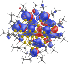
1) Graphene
As it turns out, graphene has yet another use. It has been conceptualized to use graphene as a way to protect spaceships from meteor debris and other substances that could cause corrosion of the ship. Due to its properties of being strong, flexible, cheap, and easy to make, it does not corrode, easily, thus protecting the spaceship.
(source)
Graphene sheet


Other than astronomy, this anti-corrosion property can protect objects on Earth from oxidation.

2) Space elevator
The space elevator applies carbon nanotubes to make  a shaft to let an elevator climb and get into space.
Nanotube Space elevator (artist's dipiction)
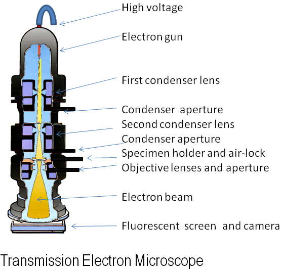
3) Telescopes: X-Rays
Wavelength of light chart
Above, is a chart that describes the wavelength of lights. Visible light is where there is the triangle  of colors in the middle of the chart. From the 10nm to the 10-3nm (10-11 meters) is a type of light called x-rays. X-rays are especially useful in astronomy. They help us take pictures of stars, detect properties of the stars and help us collect information on dark energy, black holes and neutron stars. Also, before the nanoscope was invented, it let us see things at the nanoscale, as particles at that size are to small to see with light. In other words, it lets us see things that a regular microscope can not see, like nanoparticles

However, due to the distance of the things we study in space, The changes are often very fine, and so very precise instruments are needed to detect these differences. Not only that, but the process to decipher the X-rays often takes a lot of time. 

Nanotechnologies can help by making tiny mirrors that allow scientist to use X-rays more practically and with greater precision. These mirrors can diffract light to the X-ray wavelength,thus making X-rays. The newly forged method of producing X-rays is called Critical-Angle Transmission or CAT.

4) Spaceships

The true heart and soul and astronomy is essentially astronomy.
Our current a space travels are abbord huge billion dollar investments. People are trying to make this price go down by using cheaper parts or changing design plans of the shuttle.
Saturn rocket take off
Russian Rocket ship
Shuttle rocket take off
Although these rockets seem to be totally different from each other, they have one core thing in common.

All these rockets are super-expensive projects that do not have a single mission to accomplish but a list of many tasked to accomplish while in orbit. In other words, we spend millions, if not billions of dollars to get these rockets into space to do lots of things.

There are two main things nanotechnologies can do to change this:

The first is quite obvious. Using nanotechnologies, we could make instruments on board smaller and more precise. We could also create a new type a fuel that is easier to make, cheaper, and more efficient by altering the properties of the fuel at its most basic level.


The second thing nanotechnologies could do is change the current goal of space ships. Why not create tiny little probes that do specific tasks, rather than these huge rockets that do many. It would certainly be less costly.

Even better, think about all the satellites that are in our orbit and how many are sent up each year. Now imagine that we send up a hundred or so tiny probes with each one. Each probe would the separate from the rocket, and make the rocket not only profitable to the business sending it up for business, but also profitable for science.

Monday, June 11, 2012

Copper-Nickel Nanowires

Ever wonder how the screen of an Ipad works. Me too, but I really don't know. This post, however, is just as interesting as that topic.

Copper-nickel nanowires might be the future of touch screens and for printable technologies. The nanowires are flexible and cheap and have the same properties as the current technologies in touchscreens (indium tin oxide, or ITO).

Another practical use of copper-nickel nanowires is that they can make solar panels much cheaper because it has all the necessary properties, is cheaper, and even more durable.


To start, indium tin oxide is the current leader in the field of touch screens. It is a substance that is good for touch screens because it is highly conductive (electrically) and is also transparent. However, it is rare and fairly expensive. 
Indium tin oxide glasses

A possible replacement was copper nanowires. Nanowires are wires at the nanoscale and are different from nanotubes because they are not hollow. Originally, when these nanowires were being created, it was found that after a little bit of use, the screen would actually become yellow, and then eventually green, like the statue of liberty. For obvious reasons, this type of screen was not put into commerce. However, recently at Duke University, a slight change to this original idea was made to solve some of the copper nanowire's problems.

Duke University creates the copper-nickel nanowire

Then the scientists thought about how pennies turned green, but not nickels. By adding nickel into their nanowires, they were able to take off many of the problems from the copper nanowires. One such advantage that was created by adding nickel was that it lost 50% of its conductivity in 400 years, much more than the indium tin oxide screens.Unfortunately, this new cheap alternative will probably not replace its predecessor for a simple reason; it cannot yet conduct enough electricity for our common day-to-day technologies.

Even though this is a big issue of the copper-nickel nanowires, it would be quite biased to ignore the possibilities presented with the Copper nanowires. Copper nanowires can be used in printable technologies because it is flexible, cheap, and durable. This printable technology can be used for for shipping boxes to scan it, in magazines, and much more. 
Copper Nickel Nanowires


It can also be used  as a way to make interactive clothing, which is a very tangent to this topic, but interesting none-the less.

Tuesday, June 5, 2012

Transit of Venus

Today is a big day for the opposite of nanotechnology; the study of huge things, or more specifically, astronomy.
Today, there was a transit of Venus in front of the sun. This means we got to see venus' shadow from Earth. It will be the last time for 105 years that this happens. Personally, I did not get to see it because of heavy overcast here in New Jersey, but I hoped everyone else that could enjoyed it.

Sunday, June 3, 2012

Graphene

What do we think of when we are told '2D'? Normally we think of paper or a '2D drawing', even though we know that neither paper, nor drawings are really one atom thick.

The discovery of graphene is one of the most impressive discoveries within the realm of nanotechnologies. Graphene is one atom thick, and is surprisingly easy to make. Essentially it comes from graphite, or more commonly known as pencil lead.

Gaphene is a type of carbon atoms with the formation of sp squared , which is a hexagonal formation.
Hexagonal carbon formation
Graphene is a significant discovery because it opened up the ideas, to not only 2D planes, but also 1D lines like nanotubes, and even 0D points, which are essentially atoms.

Graphene is also a big contributor to the progress of technology because of its properties. It turns out that graphene is a great conductor of electricity-its 2D qualities make electricity pass through it even faster than regular graphite, which was a good conductor to begin with. This means that it can, and will be, used in electronics to make them fast. Not only that, but it is flexible, which means it can create flexible technologies. It also is incredibly strong, even with its flexibility.

Nanogears

What is one of the most basic tool for machines to move things. The answer: Gears.
One of the newest inventions in nanotechnology, nanogears hope to create molecular-machines. They will do so in the same exact way as regular machines - just, tiny.

In the past, nanogears were created by using a laser to carve the gears. This process took up to much time to be able to get nanogears cheaply, or use them efficiently for molecular machines. Columbia university solved this problem by making nanogears that can assemble themselves. The scientist did that by putting a sheet of metal, like copper against a polymer sheet. Due to the properties of polymer, it shrinks faster than the copper sheet when it cools, thus making evenly spaced teeth in the polymer, creating a nanogears.
(Source)
However, what is the point of having these gears if they do not turn or create change? Fullerene nanogears (1st video above) are turned when a beam is sent  down the nanotube (which is what the nanogear is center is made up of) creating an electric field around the tube. "A positively charged atom is placed on one side of the nanotube, and a negatively charged atom on the other side. The electric field drags the nanotube around like a shaft turning". Source

Saturday, June 2, 2012

Contact: Dr. Anthony Novembre

Dr.Anthony Novembre
Industrial Outreach Coordinator of PCCM at Princeton University.


Anthony NovembreAssociate Director
Princeton Institute for the Science and Technology of Materials
Princeton University
70 Prospect Avenue
322 Bowen Hall
Princeton, New Jersey , 08540-5211
Phone:             609-258-6855      
Fax: 609-258-1177
Email: novembre@Princeton.edu

Contact: Daniel Steinberg

Mr. Daniel Steinberg,

Director of Education Outreach for PCCM (Princeton Center for Complex Materials) at Princeton University. Mr. Steinberg works to reach out to students at any level and get them interested in material studies.


Phone: (609) 258-5598
Email: dsteinbe@princeton.edu

Wednesday, May 30, 2012

Nanotubes

Imagine the wooden pole of an umbrella, which weighs about 4 kg and is about 2 meters tall. Now imagine a single pole like an umbrella, but hundreds of times thinner and stronger than steel. The result is nanotubes.

One square kilometer of nanotubes weighs only about 30 kilograms, it is flexible , and stronger than steel.

Due to its properties, nanotubes have become a viable candidate for a multitude of uses like strong cords to stop fighter jets when landing on a boat. One of the most famous and most anticipated uses of nanotubes is to create a space elevator that would stretch from the Earth to the moon. (Source)
Artist idea of a space elevator
Recently, researches at Rice University has discovered how to create nanotubes quickly and effectively. First they put carbon inside a furnace at 1,200 degrees Fahrenheit to heat up the carbon, and then they put the carbon through a process called laser vaporization. In essence, laser vaporizes the atoms of an object by heating it up so quickly. Then, the atoms fall back down onto the open end of the tube thus growing the nanotube. While the atoms fall onto the nanotubes ends, a catalyst of cobalt nickel prevents the tube from capping until the cobalt nickel is removed, allowing scientist to cap the nanotube at specific time, and letting them create nanotubes at specific lengths. (Source)


 Nanotubes are built up from hexagons, and because hexagons are one of the 5 platonic solids (where the enclosure of the platonic solid would create a dodecahedron). It forms a surface that has no open areas. In fact a nanotube is essentially a dodecahedron, but because of the cobalt nickel, the middle is extended until it closes. In other words, if you cut of both ends of a nanotube and put them together, you would get a dodecahedron.  (I am receiving feedback that this is not very clear, so feel free to post comment to ask questions).


It is also possible to change the nanotubes. Nanotubes are described by vectors (looks like <n,m>) that describe how far the two points that are superimposed to be rolled up are from each other. 
There are three different types of nanotubes; here are the properties of their vectors:
  • Zig-zags-the abscissa can be any number, but the ordinate is always 0
  • Armchairs-the  abscissa and ordinates are always equal
  • Chirals- is when the abscissa and ordinate have no relevance to each other, and so either can be any number 
The zig-zags and armchairs often are very symmetric while Chirals are not.
(source 1) (source 2)


Different types of nanotubes that change because of changes in vectors